By: Muydinova Madina Alisherovna
Abstract: In this article, the optical characteristics of p-n-structured photoelectric devices are strongly related to the optical properties of the surface of the material used as a base. Despite the fact that there are many types of optical layers covering the silicon surface, their use in a single and multi-layer system based on a certain physical sequence based on the value and thickness of the physical refractive index has been systematically tried by the numerical modeling method. A scientific approach to the factors of creating a photoelectric device with high efficiency from an optical point of view. Key words: refractive index, refractive index, optical property, semiconductor wafer, silicon wafer, wavelength, photoelectric device.In order to optimize the optical properties of the surface of semiconductor plates and p-p-structures built on their basis, we first refer to a number of fundamental principles. The surface of silicon wafers, which serve as the basis for photovoltaic devices, have irregularities up to several microns after they are cut from the slit using metal wires. Such surfaces of the plates are processed and polished with the help of suspensions prepared in the order of decreasing sizes of abrasive powder. The degree of smoothness of the solid surface is divided into 14 types [1]. After mechanical treatment of the surface of the silicon wafers, the surface is washed and chemically treated. On the surface of the plates there will be irregularities called fine textures. The optical characteristic of the surface of the plates is mainly understood as the optical reflection coefficient of the light falling on the surface and its dependence on the wavelength of the light falling on it. The reflection coefficient R and the refractive index n of the plates also depend on the wavelength of the light. Usually, when talking about the reflection coefficient or refractive index values of the surface of a solid body, the case when the wavelength of the light is 0.5 µm is meant. The optical properties of the surface are measured using monochromators. In this case, using different optical schemes, the light sent to the surface of the solid body, the light reflected from it, and the light fluxes passing through the plate are realized by using the same photosensors for different incidence angles and different thicknesses of the plates. When measuring the optical characteristics of the surface of the plates intended for photoelectric devices, monochromators capable of separating rays of 0.3 ÷ 1.1 μm wavelength are used.It is possible to increase the optical efficiency of the photoelectric device by forming optical traps that capture the light beam on the front or back side [2]. Figure 1 shows a graph showing such a situation.
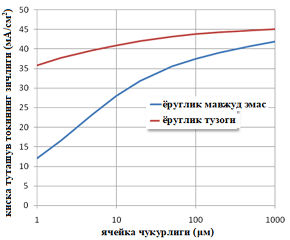
Figure 1. Distribution of short-circuit current through thickness in a silicon-based structure with and without a special light-trapping grating.
By comparing the graphs in Figure 1, it can be seen that the thickness of the silicon wafer can be partially reduced if the optical traps are formed.
The characteristics of the plates serving as the basis for the photoelectric device, including optical, are significantly affected by their alloying level. In this work [3] silicon-based n+-p-p+ structured photoelectric devices were tested under the influence of 7 MeV electron flow. The change in the residence time of charge carriers (charge carriers) has been considered as a factor that reduces the efficiency of photovoltaic devices.
An important aspect of the work is that the factors that can affect the value of the charge carrier lifetime are the detection of defects in the silicon volume. A useful aspect of this work is the confirmation of the dependence of the carrier lifetime on the doping level and defect concentration in silicon. In other words, the correctness of the graph presented in Figure 2 was confirmed in this work. in order for the efficiency of the photoelectric device to be high, the charge carrier residence time or their diffusion length on the silicon plate must be large enough, or the doping level must not exceed a certain standard.
Figure 2 shows the influence of the doping level of the silicon wafer on the diffusion length of charge carriers and the operating voltage of photoelectric devices based on it [4]. It can be seen from the graph that if the doping level of the base is more than 1017 sm-3, the charge carrier diffusion length starts to decrease sharply. The operating voltage of a photoelectric device based on such a plate reaches a maximum at that limiting concentration and decreases at higher concentrations.
It should be noted that, usually, the emitter layer of a photoelectric device has a concentration 1-2 orders of magnitude higher than the base. Therefore, it is prepared in a very thin form.
Active photogeneration of charge carriers usually occurs in the base region. The emitter and the volume charge region of the p-p junction are active recombination regions. In order to reduce bulk recombination, an internal isotype field is formed within the base near the back of the photoelectric device. In order to reduce recombination processes, passivating optical layers are covered on the frontal and rear surfaces.
In the isotype field generated work, a double photosensitive photoelectric device with n+-Si/n-Si/SiO2/n+-ITO structure was developed. The advantage of such photoelectric devices is that they are obtained by a technologically simpler pyrolytic pulverization method and it does not matter at what angle the light beam falls.
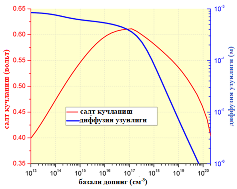 Figure 2. Dependence of the diffusion length of non-primary charge carriers in the silicon p-p structure and the degree of doping of the operating voltage.
Anti-reflection layers are used on the silicon wafer in order to reduce the reflection of light and the recombination process. The refractive index of the optical layers used for this purpose should have a value between the refractive indices of silicon (n=3.4) and air (p=1). In the application of such a layer as an anti-reflection layer, the laws of interference play a key role in the overlap of optical rays returning from the boundary surfaces of the first – “air / anti-reflection layer” and the second – “anti-reflection layer / silicon”. The thickness of the anti-reflection layer should be such that the interference minimum condition for the light returning to the air must be met.
Various optically transparent materials are used as an anti-reflection layer. In the scientific literature, there is information about the use of mainly single-layer and partially double-layer anti-reflection layers. But multilayer structures have not been studied in detail.
The influence of the transparency and electrical conductivity indicators of different thicknesses of some optical materials on the efficiency of the photoelectric device has hardly been studied.
One of the ways to improve optical properties of semiconductor material, plate surface or photoelectric device surface is texturing.
Textures can be very different depending on different nature, different geometric shapes and sizes, as well as uniformity or non-homogeneity in distribution on the surface and technologies of their formation [6]. In the information provided in the scientific articles, it can be seen that usually only one type of texture is used for photoelectric devices with a certain base and structure, and optimization measures are taken for this particular case. However, photoelectric devices on the same basis with the same types of textures and anti-reflective layers on top of them have hardly been studied in a complex manner.
Therefore, the optical characteristics of p-p-structures and photoelectric devices are strongly related to the optical properties of the surface of the material used as a base. Despite the fact that there are many types of anti-reflection layers covering the silicon surface, their use in a single and multilayer system depending on the value and thickness of the physical refractive index has not been systematically studied by numerical modeling.
Also, research on texturing and the use of additional anti-reflective coatings has not been integrated into one system. In order to create a photoelectric device with high efficiency from an optical point of view, first – to select a semiconductor material based on light absorption characteristics; secondly, the thickness of the semi-conducting material, and thirdly, the quality of its surface treatment; fourthly, factors such as surface defects and the passivation of various states leading to the recombination of photogenerated charge carriers require a scientific approach. That is, conducting scientific research aimed at improving the optical efficiency of photoelectric devices as much as possible is one of the urgent tasks.